Crystals Process and Production at Photonics On Crystals (POC)

Photonics On Crystals (POC) specializes in advanced crystal processing and mass production, offering state-of-the-art solutions for optical and photonics industries with unparalleled precision and expertise.

Expanded Capabilities:

With years of expertise, POC delivers end-to-end solutions, including crystal growth, cutting, coating, and optical processing, ensuring customized products and services tailored to the precise needs of industries such as medical, defense, and scientific research. Specifications and Features: Crystal sizes from 1 mm to 180 mm in diameter.
Precision surface flatness up to λ/10 @ 632.8 nm.
Wide array of coatings tailored to customer needs.
Fast delivery starting from one week, with customization options available.

Metrology and Quality Assurance:

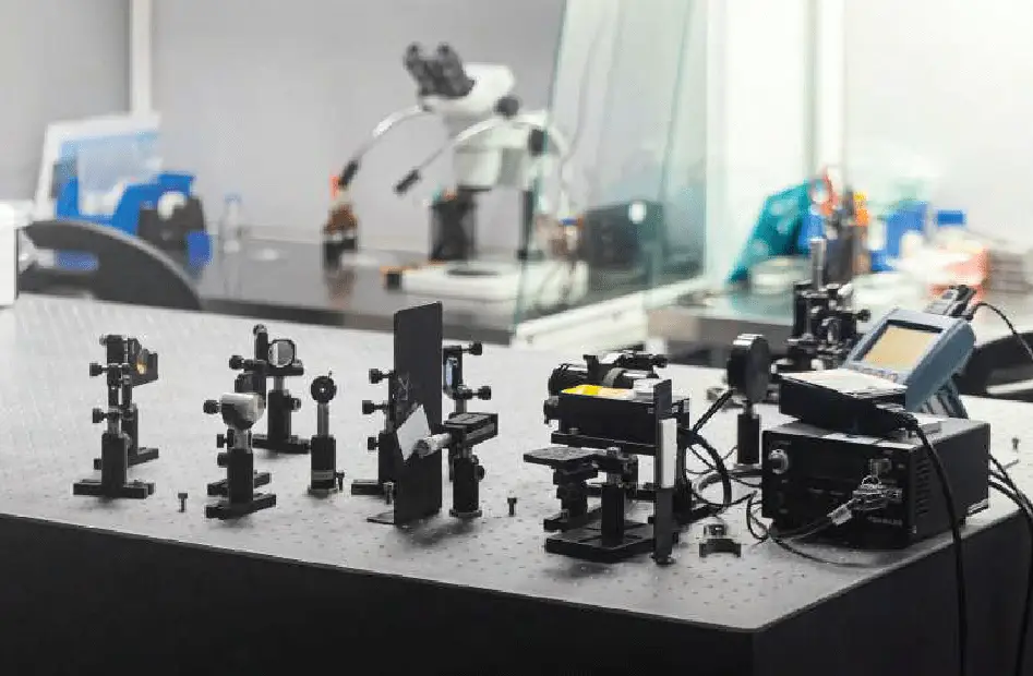
Our in-house metrology ensures product reliability and quality with advanced equipment like Zygo interferometers and Olympus microscopes. POC performs detailed tests, including: Wavefront distortion measurements.
Transmittance and reflectance analysis across 200–1700 nm.
Beam quality and stability assessments.
Environmental durability tests for coatings.

1. Crystal Growth

  • Material Selection: The process begins with selecting the right crystal material, such as calcium fluoride (CaF₂), quartz, zinc sulfide (ZnS), sapphire (Al₂O₃), or others depending on the application.
  • Growth Techniques:
    • Czochralski Method: Used for growing single crystals like silicon or sapphire by slowly pulling a seed crystal from a molten material.
    • Bridgman-Stockbarger Technique: Used for growing bulk crystals by gradually cooling molten material in a controlled manner.
    • Hydrothermal Growth: Used for growing crystals like quartz under high pressure in a water solution.
    • Chemical Vapor Deposition (CVD): Used for creating polycrystalline materials like ZnS or ZnSe.

2. Cutting and Shaping

  • The grown crystal is cut into raw blanks using diamond saws or laser cutting techniques.
  • The blanks are shaped into desired geometries, such as lenses, prisms, or windows, based on the optical system’s design requirements.

3. Annealing

  • Crystals undergo a heat-treatment process to reduce internal stresses and defects, improving optical performance and stability.

4. Polishing

  • Surfaces are polished to achieve a high degree of flatness and surface smoothness, typically measured in terms of surface roughness and flatness in nanometers.
  • Techniques like lapping and chemical-mechanical polishing (CMP) are used to meet the desired optical specifications.

5. Coating

  • The crystal surfaces are coated with thin films to enhance optical properties. Coating processes include:
    • Anti-Reflective (AR) Coating: Reduces surface reflections and improves transmission.
    • High-Reflective (HR) Coating: Enhances reflectivity for laser mirrors.
    • Diamond-Like Carbon (DLC) Coating: Improves durability and resistance to harsh environments, often for infrared optics.
  • Coatings are applied using techniques like vacuum deposition, electron-beam evaporation, or sputtering.

6. Inspection and Testing

  • The finished crystal undergoes rigorous quality control to ensure compliance with optical specifications. Methods include:
    • Interferometry: Measures surface accuracy and wavefront distortion.
    • Spectrophotometry: Verifies transmission and reflection properties.
    • Scratch-Dig Testing: Assesses surface defects.
    • Stress Birefringence Testing: Checks for internal stresses.

7. Final Assembly and Packaging

  • The optical crystals are integrated into devices or assemblies as needed.
  • Crystals are carefully cleaned, inspected, and packaged in protective environments to prevent contamination or damage during transportation.