I. Introduction
Photonic Integrated Circuits (PICs) are revolutionizing fields such as telecommunications, quantum computing, and biomedical imaging through rapid improvements in data transmission rates, integration density, and compatibility with CMOS fabrication. These advancements offer exceptional scalability and efficiency.
A major challenge, however, lies in the integration of III-V compound semiconductor lasers into Silicon PICs (SiPICs). The key difficulty is aligning the PIC waveguide with the laser waveguide, which typically operates on a micron scale. While silicon offers numerous advantages for electronics, it is less effective for light emission due to its indirect bandgap. III-V materials, known for their excellent light-emitting properties, are well-suited for overcoming this limitation.
Traditionally, III-V lasers are integrated into SiPICs using techniques such as:
- Hybrid pick-and-place transfer
- Heterogeneous or monolithic integration
- Coupling via optical fibers from external laser modules
II. Integration Methods of III-V Lasers into SiPICs
Monolithic Integration
This approach involves growing III-V layers directly on silicon wafers. It provides high alignment precision but lacks the ability to test laser performance before integration. The high temperatures involved may also conflict with standard CMOS processes, complicating compatibility with silicon electronics.
Heterogeneous Integration
This method bonds unpatterned III-V dies onto silicon waveguides using wafer-scale lithographic alignment. Although suitable for large-scale production, it demands a very clean, strain-free bonding surface. Any contamination or stress can significantly impact performance.
Hybrid Integration
In this method, pre-fabricated III-V lasers are bonded onto or next to the silicon substrate. It preserves the laser’s native performance and allows for pre-integration testing. However, it introduces difficulties in optical alignment and coupling efficiency. Additional components like micro-lenses or prisms are often needed, which increase complexity and thermal management challenges—especially due to the poor heat conduction between III-V materials and silicon (often separated by a buried oxide layer).
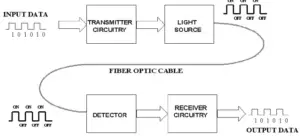
III. Photonic Wire Bonding (PWB)
Photonic Wire Bonding (PWB) emerges as a promising hybrid integration strategy. It uses 3D-printed polymer waveguides to create direct optical links between photonic components, regardless of material or structural mismatches. PWB enables flexible, accurate, and compact interconnections, reducing complexity and improving performance.
One of PWB’s standout features is wavelength tunability. This allows a single laser to serve multiple WDM channels, lowering system costs and minimizing the need for multiple discrete lasers.