Integrating photonics and electronics can significantly enhance system performance, reduce costs, and unlock new design opportunities. There are two primary approaches to achieving this integration: monolithic and multi-chip integration.
Monolithic Integration
Monolithic integration involves fabricating photonic and electronic components together in a single process flow. A pioneer in this area, Luxtera, developed a CMOS-photonics foundry process based on a 130 nm CMOS platform. Luxtera, in collaboration with ST Microelectronics, launched the first silicon photonics product in the market. In their process, CMOS transistors continue functioning alongside added components like germanium photodetectors and silicon etches for waveguides.
This integration has required substantial process development, incorporating additional layers to maintain compatibility with existing CMOS technologies. However, a critical challenge lies in integrating III-V materials (used in photonics) with the standard CMOS process, given the cost, yield issues, and other constraints. Another approach, proposed by IHP, focuses on integrating bipolar transistors with silicon photonics, a promising development that remains under exploration.
Multi-Chip Integration
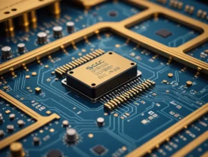
In contrast, multi-chip integration involves bonding photonic and electronic components from different processes onto the same substrate, connected electrically. Depending on the application, the photonic chip may be placed on top of or beneath the electronics chip. Proven techniques, such as wire-bonding, flip-chip bump bonding, and through-silicon vias (TSV), help reduce parasitic capacitance and increase device density.
The benefits of multi-chip integration are substantial. As CMOS technology continues to advance with Moore’s law, it becomes easier to bond successive generations of CMOS or Bi-CMOS onto inexpensive silicon photonics wafers. This allows for the use of optimized photonic and electronic processes without needing to fabricate very small photonic structures.
This multi-chip approach is expected to play a significant role in the future of silicon photonic research and product development, particularly due to the flexibility it offers for integrating cutting-edge electronic technologies.


