Our company provides end-to-end solutions—from crystal growth and cutting to coating and optical processing—offering customized products for medical, defense, and scientific applications.
Specifications and Features:
- Crystal sizes from 1 mm to 180 mm in diameter
- Precision surface flatness up to λ/10 @ 632.8 nm
- Wide array of coatings tailored to customer needs
- Fast delivery starting from one week (customization available)

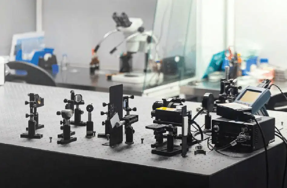
Our in-house metrology ensures product reliability and quality with advanced equipment like Zygo interferometers and Olympus microscopes. Detailed tests will be performed, including:
- Wavefront distortion measurements
- Transmittance and reflectance analysis across 200–1700 nm
- Beam quality and stability assessments
- Environmental durability tests for coatings
The process starts with selecting suitable crystal materials—such as CaF₂, ZnS, quartz or sapphire—based on the application. Crystals are then grown using methods like Czochralski, Bridgman-Stockbarger, hydrothermal, or CVD, depending on the desired properties.
The grown crystal is cut and shaped into optical blanks—such as lenses, prisms, or windows—according to design requirements.
Crystals undergo a heat-treatment process to reduce internal stresses and defects, improving optical performance and stability.
Surfaces are polished using lapping or CMP to achieve nanometer-level flatness and smoothness.
The finished crystal undergoes quality control using interferometry, spectrophotometry, scratch-dig, and birefringence tests to ensure it meets optical specifications.
Optical crystals are integrated into devices, then cleaned, inspected, and securely packaged to prevent contamination or damage.
Crystal surfaces are coated with thin films—such as AR, HR, or DLC coatings—to enhance optical performance and durability, using methods like vacuum deposition, e-beam evaporation, or sputtering.