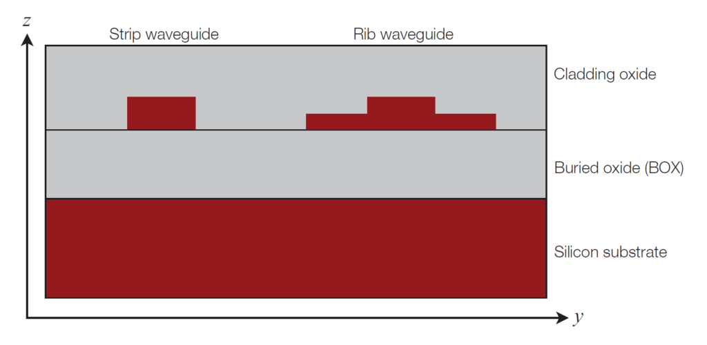
Several types of waveguides are used in silicon photonics, primarily the strip waveguide (also referred to as channel waveguide, photonic wire, or ridge waveguide) and rib waveguide. Strip waveguides are commonly used for routing due to their ability to support tight bend radii, making them ideal for applications like optical interconnects. Rib waveguides are suitable for electro-optic devices such as modulators since they allow for the integration of electrical connections with the optical waveguide. Both waveguide types can be fabricated to achieve a loss of less than 3 dB/cm. Oxide cladding protects devices and supports the creation of metal interconnects above waveguides. In specific designs like evanescent field sensors, waveguides can be fabricated without cladding for lab-on-chip applications.

Waveguide Design: Key Steps
- One-Dimensional (1D) Mode Calculation: The process starts with 1D calculations of slab waveguide modes, supported by the material layer and wafer (e.g., with oxide cladding). The silicon thickness is determined based on the requirement for supporting only a single transverse electric (TE) and transverse magnetic (TM) waveguide mode. A common thickness used in silicon-on-insulator (SOI) systems is 220 nm, though other options like etched silicon with a thickness of 90 nm are also used.
- Waveguide Width Optimization: The waveguide width is selected to match the given silicon thickness. The width is optimized to support a single TE and TM waveguide mode. Methods like the effective index method (EIM) or fully vectorial 2D simulations are used to determine the optimal width.
- Additional Considerations: Designers must consider aspects like waveguide bend loss and substrate leakage. These factors affect the overall performance of the waveguide and need to be minimized.
Simulation and Analysis: The final waveguide properties, such as the effective index, mode profile, and group index, are computed using simulations to optimize the design.


