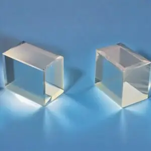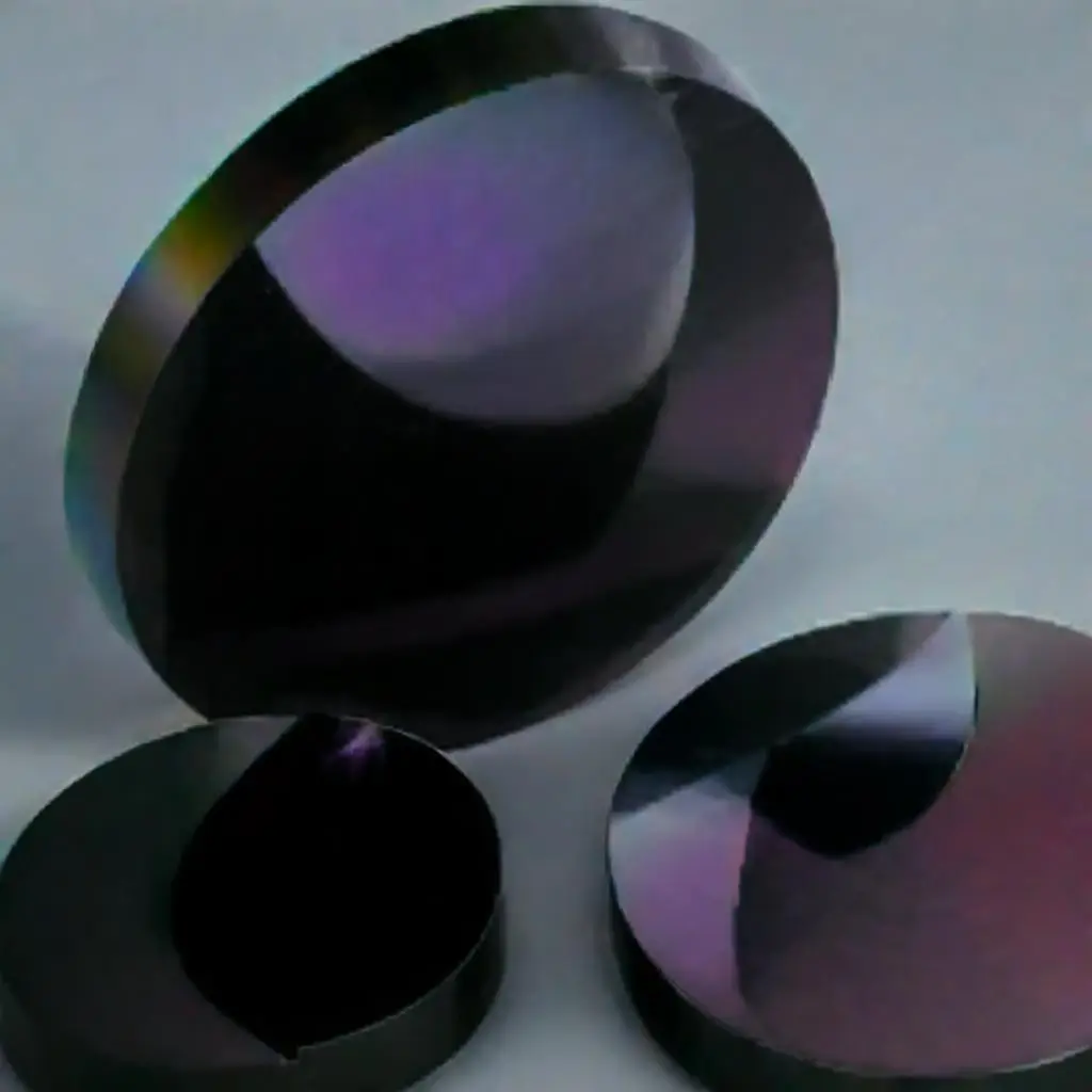
Silicon single crystal is a highly durable material known for its excellent optical transmission in the infrared spectrum, spanning from 1 to 7 μm. Its unique property of transparency in the far-infrared range (30-300 μm) makes it an ideal choice for specialized optical components. The material is commonly used in mid-wave infrared (MWIR) optical systems due to its outstanding transmission and minimal absorption. The crystalline structure is strong and insoluble in water, ensuring stability and robustness for demanding applications. Thanks to its high thermal conductivity and low density, silicon crystals are also utilized in laser mirror substrates and filters.
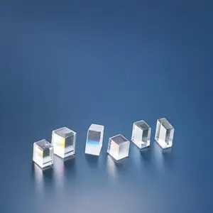
Silicon crystals find extensive applications across diverse scientific and industrial fields due to their exceptional optical and thermal properties:
| Property | Specification |
|---|---|
| Material Grade | CZ, FZ; Intrinsic Silicon |
| Max Crystal Size | Ø300 mm |
| Growing Method | CZ/FZ |
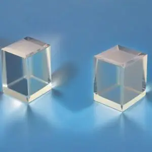
| Crystal Structure | Monocrystalline |
| Type | N-type/P-type |
| Cleavage Planes | <111> |
| Density | 2.33 g/cm³ |
| Thermal Conductivity | 148 W/m·K |
| Thermal Expansion | 2.6 × 10^-6 /K |
| Mohs Hardness | 7 |
| Melting Point | 1,410°C |
| Specific Heat Capacity | 700 J/kg·K |
| Optical Property | Specification |
|---|---|
| Transmittance Range | 1.2-15 μm |
| Transmittance | >95% in the 1-6 μm range |
| Refractive Index | 3.42 (at 1.5 μm) |
| Absorption Coefficient | 10^-3 @10.6 μm |
| Thermal Lens Effects | Negligible for standard power |
| Laser Damage Threshold | >10 J/cm² @1064 nm, 10 ns |
| Specification | Details |
|---|---|
| Flatness | λ/8 @632.8 nm |
| Parallelism | <1 arcmin |
| Surface Quality | 40-20 (scratch-dig) |
| Clear Aperture | >90% |
| Bevel | <0.25 mm × 45° |
| Length Tolerance | ±0.1 mm |
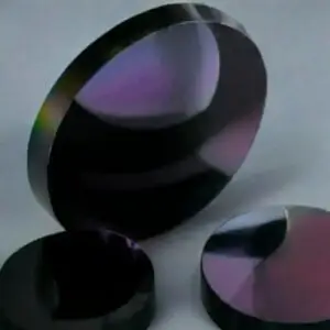
| Coating Options | Customizable as per user request |
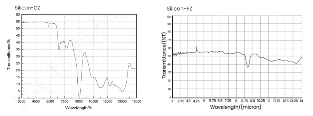
Two transmission curves are provided:
| Coating Type | Wavelength Range | Reflection Loss | Durability |
|---|---|---|---|
| Standard AR Coating | 1-7 μm | <0.5% | Scratch-resistant |
| Custom Coating | On demand | <0.3% | High durability |
| Product | Dimensions | Coating | Price (USD) |
|---|---|---|---|
| Silicon Window | Ø100 mm | AR (1-7 μm) | 300 |
| Silicon Lens | Ø50 mm | AR (3-5 μm) | 150 |
| Custom Silicon Parts | On request | Custom Coating | Based on spec. |