
Introduction
The rapid advancement of photonics bonding is driving a new era in optical interconnects, enabling high-speed, high-density integration of photonic devices. As the demand for photonic integrated circuits (PICs) grows, the need for seamless, low-loss, and scalable optical connections has never been greater. Photonics bonding provides a breakthrough solution, facilitating precise and efficient coupling between optical chips, fiber arrays, and laser sources, overcoming the limitations of conventional packaging and assembly methods.
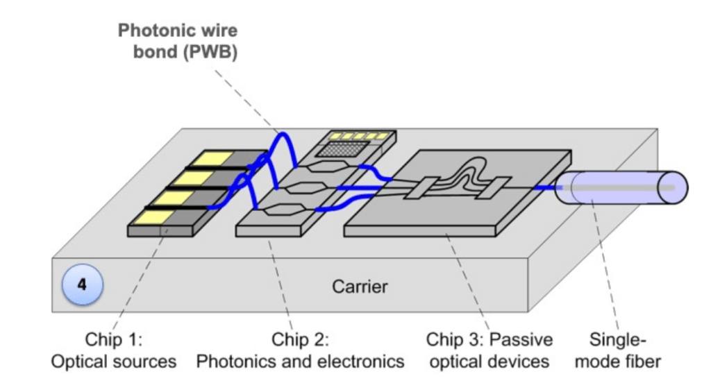
What is Photonics Bonding?
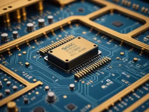
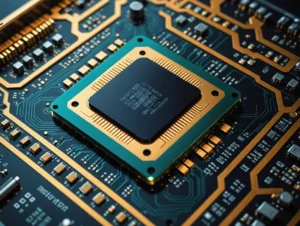
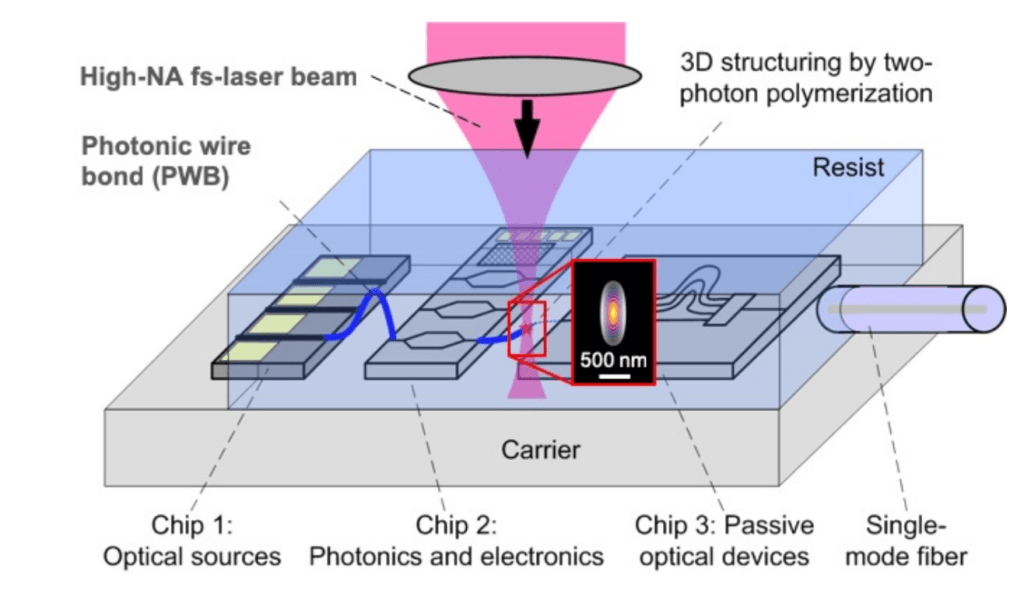
Photonics bonding is a cutting-edge manufacturing technique that utilizes additive 3D nanofabrication to create freeform optical waveguides, connecting various photonic components with minimal insertion loss. This technology allows photonic devices to be interconnected seamlessly while maintaining high efficiency.
Key Features
- Flexible Optical Interconnects: Customizable 3D-printed waveguides for diverse optical applications.
- Low-Loss Coupling: Significantly reduces optical losses compared to traditional fiber-based alignment techniques.
- High Scalability: Enables large-scale integration of photonic chips with minimal footprint.
- Automated and Passive Alignment: Eliminates the need for expensive active alignment processes.
Working Principle
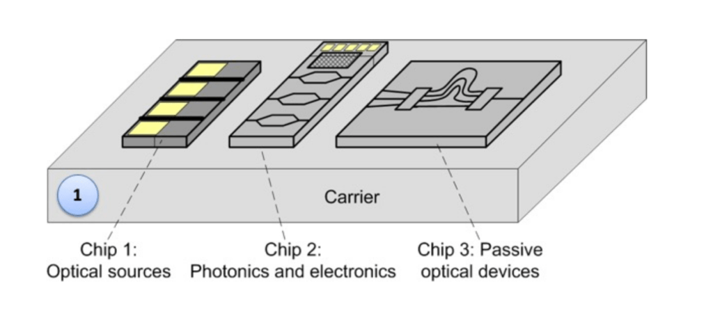
Component Placement: Photonic chips and fiber arrays are pre-positioned using precision placement systems.
3D Printing of Optical Waveguides: The photonic interconnects are fabricated using high-resolution laser lithography
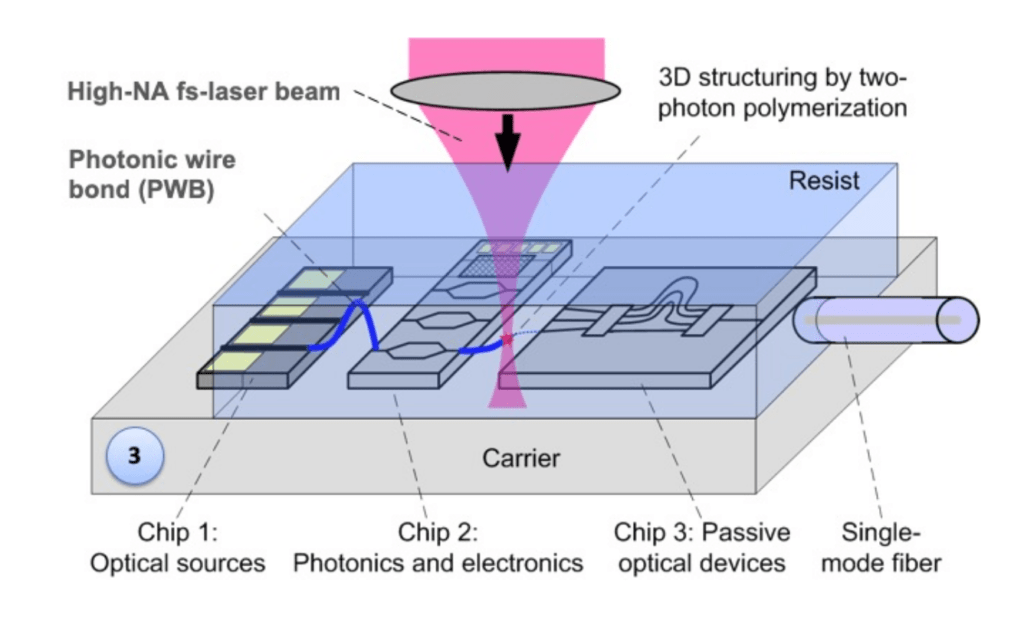
Waveguide Optimization: Mode-matching structures are integrated to enhance optical efficiency.
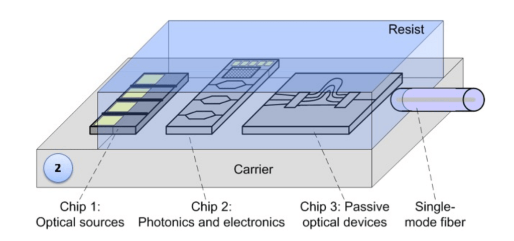
Encapsulation and Finalization: The bonded photonic assembly is protected and optimized for long-term performance.
Applications of Photonics Bonding
1. Advanced Photonic Packaging
Photonics bonding enables hybrid integration of InP-based lasers, silicon photonic modulators, and fiber arrays, optimizing high-speed data transmission in telecom, datacom, and sensing applications.
2. Optical Interconnects for Data Centers
With increasing bandwidth demands, photonics bonding enhances optical transceiver performance in 400G and 800G networks, reducing insertion loss and ensuring seamless signal transmission.
3. High-Precision Fiber-to-Chip Coupling
Photonics bonding improves coupling efficiency by leveraging mode-matching structures, reducing optical losses and enhancing the stability of fiber-to-chip interconnects.
Advantages of Photonics Bonding
| Feature | Benefit |
|---|---|
| Ultra-Low Optical Loss | Enhances signal transmission and minimizes power loss |
| Compact and Scalable | Supports dense photonic integration for next-gen devices |
| Automated Alignment | Reduces manufacturing complexity and costs |
| High Versatility | Compatible with various photonic materials (SiPh, InP, LiNb, etc.) |
Photonics bonding is revolutionizing the optical industry by providing an efficient, scalable, and low-loss solution for photonic interconnects. With applications in high-speed data transmission, quantum computing, and optical sensing, this technology is paving the way for the next generation of photonics manufacturing and integration. As the demand for high-performance optical interconnects continues to rise, photonics bonding is set to become a fundamental enabler in the evolution of photonic systems.