
Introduction
The demand for high-speed, high-density optical interconnects in photonic integrated circuits (PICs) has led to the development of advanced packaging solutions. Photonic Wire Bonding (PWB) is a cutting-edge technique that enables precise and efficient coupling between optical components, overcoming the scalability limitations of traditional fiber-based or free-space interconnects. This technology allows seamless integration of multi-chip photonic modules, significantly improving performance and reducing alignment complexity.
What is Photonic Wire Bonding?
Photonic Wire Bonding (PWB) is an additive manufacturing technique that fabricates freeform optical waveguides directly between optical components. These wire bonds act as low-loss optical interconnects, allowing efficient coupling between different photonic chips, fiber arrays, and laser sources.
Key Features of PWB
- Freeform Optical Interconnects: PWBs are printed in situ, enabling flexible, three-dimensional waveguide paths between components.
- High Coupling Efficiency: Reduces optical losses compared to traditional alignment-based fiber coupling.
- Scalability: Facilitates integration of multiple photonic components in a compact footprint.
- Passive Alignment Tolerance: Overcomes the need for high-precision, active alignment techniques.
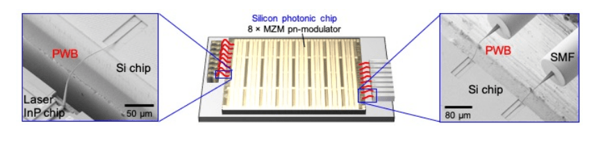
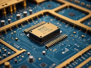
The multi-chip module consists of an 8 x laser array on an InP chip, an 8 × MZM pn-modulator on a silicon photonic chip (SiP), and 8 x single mode fibers (SMF) fixed on a common carrier and all connected with photonic wire bonds (PWBs).
Working Principle
- Pre-Alignment and Printing: Optical chips and components are pre-positioned on a common substrate or carrier.
- 3D Nanoprinting Process: A high-resolution 3D printing system fabricates photonic waveguides that connect the components.
- Waveguide Optimization: The printed structure is optimized for low loss and high mode-matching between connected elements.
- Final Integration: The bonded photonic circuit is encapsulated and tested for performance.
Applications of PWB
1. Multi-Chip Photonic Integration
PWB allows seamless integration of hybrid photonic chips such as InP-based laser arrays, silicon photonic modulators, and fiber arrays. This integration is essential for high-speed transceivers and optical computing.
2. Optical Transceivers
The use of PWBs in 400G and 800G photonic transceivers reduces insertion loss and footprint while enabling high-bandwidth data transmission. These transceivers leverage the scalability of PWBs to integrate multiple optical channels with minimal power loss.
3. Fiber-to-Chip Coupling
PWBs improve fiber-to-chip interconnects by providing mode-matched transitions, reducing insertion losses, and enabling compact photonic packaging.
Advantages of PWB
| Feature | Benefit |
|---|---|
| Low Optical Loss | Minimizes insertion loss compared to fiber-based coupling |
| Compact Footprint | Enables denser integration of photonic components |
| Scalability | Facilitates high-channel count systems |
| Passive Alignment | Reduces manufacturing complexity |
| Versatile Connectivity | Supports hybrid photonic integration (SiPh, InP, LiNb, etc.) |
Conclusion
Photonic Wire Bonding is revolutionizing the way optical components are interconnected in next-generation photonic systems. By enabling low-loss, scalable, and flexible optical interconnects, this technology is unlocking new possibilities for high-speed data transmission, optical computing, and quantum photonics. As the industry moves toward heterogeneous photonic integration, PWBs will play a crucial role in shaping the future of optical communication.